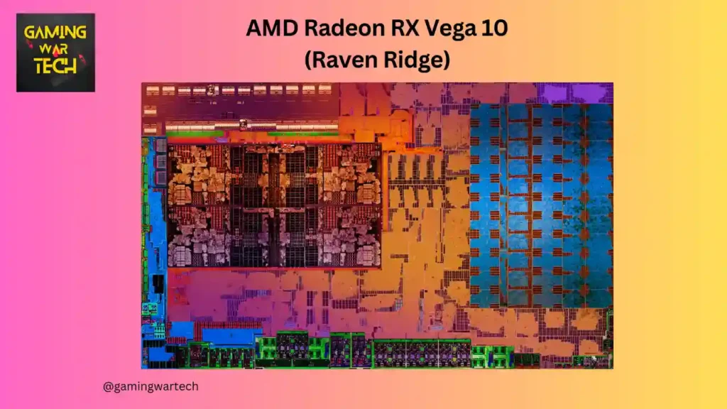
AMD Radeon RX Vega 10 (Raven Ridge) is an integrated graphics for Ryzen 2000 series laptop APUs launched on Oct 26th, 2017 and the PRO version was launched on Jan 8th, 2019.
Later on Jan 6th, 2019; the refresh of Raven Ridge, RX Vega 10 Picasso was released for Ryzen 3000 series laptop and desktop APUs.
I have collected all the data from reputable sites like Techpowerup, Notebook-Check, etc. for the specs and performance of the integrated AMD Radeon RX Vega 10 graphics.
Let’s dive into all the capabilities, specs, benchmarks, and gaming performance of the RX Vega 10 graphics.
AMD Radeon RX Vega 10 (Raven Ridge) Info
All the basic information about the Radeon RX Vega 10 GPU is presented such as GPU Architecture, market segment, codename, and price.
| GPU Codename | Raven Ridge |
| Architecture | GCN 5.0 |
| Release date | Oct 26th, 2017 |
| Generation | Vega IGP |
| Foundry | GlobalFoundries |
| Market Segment | Laptop |
| Production | Active |
| Predecessor | GCN 3.0 IGP |
| Successor | Navi II IGP |
| Price | No Data |
Technical Specifications
AMD Radeon RX Vega 10 Specs include compute units, number of shaders, pixel rate, texture filter rate, die size, density, TDP, process size, Vram, and more.
| Compute Units | 10 CUs |
| Shaders / Stream Processors | 640 Units |
| TMUs (Texture Mapping Units) | 40 |
| ROPs (Raster Operation Pipeline) | 8 |
| RayTracing Cores | None |
| L1 Cache | No Data |
| L2 Cache | No Data |
| Transistors | 4.94 billion |
| Process Size | 14 nm |
| Die Size | 210 mm² |
| Density | 23.5M / mm² |
| Chip Package | FCBGA-1140 (FP5) |
| Pixel Rate | 10.40 GPixel/s |
| Texture Rate | 52.00 GTexel/s |
Board Design
| TDP (Total Draw Power) | 10 W (Up to 15W) |
| Slot Width | IGP |
| Outputs | Portable Device Dependent |
| Bus Interface | IGP |
| Power Connectors | None |
GPU Frequencies
The AMD Radeon graphics RX Vega 10 mobile is clocked at 1.3 GHz.
| Base Clock | Boost Clock | FP16 (Half) | FP32 (Float) | FP64 (Double) |
|---|---|---|---|---|
| 300 MHz | 1.30 GHz | 3.328 TFLOPS | 1.664 TFLOPS | 104 GFLOPS |
Video Memory (VRAM) capacity and Type
It tells how much VRAM Radeon RX Vega 10 GPU has, VRAM type, size, bus, and bandwidth. Since this is an i-GPU, it doesn’t have a dedicated VRAM and uses a part of the system RAM.
The Radeon RX Vega 10 VRAM allocation max. capability is only 1GB, which can be increased via BIOS.
| Memory Size | System Shared |
| Memory Type | System Shared |
| Memory Bus | System Shared |
| Memory Clock | System Shared |
| Bandwidth | System Dependent |
API Features Support
Graphical API features supported by AMD Radeon RX Vega 10 Ryzen 2000 graphics card are:
| DirectX | 12 (12_1) |
| OpenGL | 4.6 |
| OpenCL | 2.1 |
| Vulkan | 1.3 |
| Shader Model | 6.7 |
Other Hardware Features
| Multi-Monitor Support | Yes (up to 3) |
| Max. Resolution | 1920×1080 @ 60Hz |
| AMD FreeSync | Yes |
Hardware Codec Support
Hardware codecs supported by this GPU are:
| h264 | Decode / Encode |
| AV1 | No |
| h265 / HEVC (8-bit) | Decode / Encode |
| h265 / HEVC (10-bit) | Decode / Encode |
| VP8 | Decode / Encode |
| VP9 | Decode / Encode |
| VC-1 | Decode |
| AVC | Decode / Encode |
| JPEG | Decode / Encode |
Synthetic Benchmark Performance
These benchmarks are measured by GPU benchmarking software like 3DMark Time Spy graphics score, 3DMark Fire strike graphics, Passmark Performance Testsuite, and Geekbench 6.2.
What is the Passmark Performance Test suite?
The Passmark performance test suite is a 3D benchmark designed for video cards by using the DirectX feature.
It puts a load on the GPU for various DirectX versions like DX9, DX10, DX11, and DX12 provides separate benchmark results, and gives you the average G3D mark score.
What is the 3D Mark Time Spy benchmark?
It calculates both the CPU and GPU performance and gives you the system’s overall score. It also ranks your overall score on the internet and ranks your system accordingly.
What is the 3D Mark Fire Strike benchmark?
It is a standard to test your gaming PC graphics render capability in detail and complexity which is quite taxing to the gaming hardware. It uses DirectX 11 API and renders at 1080P resolution.
What is the Geekbench 6 GPU benchmark?
Geekbench 6 GPU benchmarks your graphics card computing power in gaming, image processing, video editing, photography, and machine learning. It tests your GPU Open CL, metal, and Vulkan score.
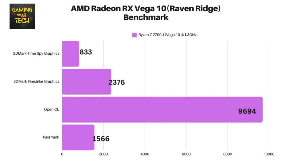
| Benchmark Tools | Ryzen 7 2700U (Radeon RX Vega 10 at 1.3 GHz) |
|---|---|
| 3DMark Time Spy Graphics | 833 |
| 3DMark Firestrike Graphics | 2376 |
| Open CL | 9694 |
| Vulkan | No Data |
| Passmark | 1566 |
RX Vega 10 Gaming Performance
Gaming performance is to measure how well this integrated graphics card performs in gaming by running multiple games on it and calculating the average fps and 1% lows.
Gaming Benchmark on AMD Radeon RX Vega 10 GPU on Ryzen 7 2700U
The gaming benchmark is from the Ryzen 7 2700U integrated GPU, which is Radeon RX Vega 10 clocked at 1.30 GHz.
The Test System is a HP EliteBook 735 G5 3UN62EA with Ryzen 7 2700U and onboard Radeon RX Vega 10 graphics, 16GB DDR4 RAM, and Win 10.
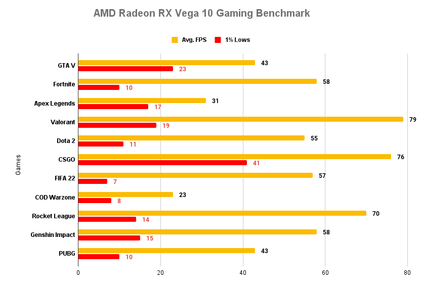
Gaming benchmark details in table format
| Games | Avg. FPS | 1% Low | Graphics Setting |
|---|---|---|---|
| GTA V | 43 | 23 | 720p, Normal |
| Fortnite | 58 | 10 | 1080p, Low, 80% Res. Perf. Mode |
| Apex Legends | 31 | 17 | 720p, Low |
| Valorant | 79 | 19 | 1080p, Low |
| Dota 2 | 55 | 11 | 1080p, Low |
| CSGO | 76 | 41 | 720p, Low |
| FIFA 22 | 57 | 7 | 1080p, Low |
| COD Warzone | 23 | 8 | 720p, Low |
| Rocket League | 70 | 14 | 900p, Perf |
| Genshin Impact | 58 | 15 | 1080p, Low, 60% Res |
| PUBG | 43 | 10 | 720p, V. Low, 70% Res. scale |
Is AMD Radeon Vega 10 graphics good for gaming?
Rx Vega 10 can only play games at 720p/900p low settings. 1080p gaming is worse. Modern AAA titles can’t run even on 720p/900p low but with FSR, the playable framerate of 30-45 FPS is possible.
What is the Radeon RX Vega 10 Nvidia equivalent?
Radeon RX Vega 10 easily beats the Nvidia MX110 mobile dedicated GPU and is equivalent to the Nvidia Geforce MX 130 in terms of performance.
AMD Radeon RX Vega 10 (Raven Ridge) GPU Used in the Following CPU
| Processors | GPU Base Clock | GPU Boost Clock | FP32(Float) |
|---|---|---|---|
| Ryzen 7 2700U | 300 MHz | 1.25 GHz | 1.760 TFLOPS |
| Ryzen 7 PRO 2700U | 300 MHz | 1.30 GHz | 1.830 TFLOPS |

