AMD Radeon Vega 7 (Barcelo) is an integrated graphics for Ryzen 5000/7000 U series laptop/notebook APUs launched on Jan 6th, 2022. It is also known as AMD Radeon graphics 448SP (Ryzen 5000/7000).
A Cezanne refresh known as “Barcelo” is used in Ryzen 5 5000U series APUs and Later on Jan 4th, 2024, a “Barcelo Refresh” was launched for Ryzen 5 and Ryzen 7 7000U series APUs.
I have collected all the data from reputable sites like Techpowerup, Notebook-Check, etc. for the specs and performance of the Radeon RX Vega 7 integrated graphics.
Let’s dive into all the capabilities, specs, benchmarks, and gaming performance of the AMD Radeon graphics (igpu) 7cu/448SP.
AMD Radeon RX Vega 7 (Barcelo) Info
All the basic information about the Radeon RX Vega 7 GPU is presented such as GPU Architecture, market segment, codename, and price.
| GPU Codename | Barcelo/Barcelo Refresh |
| Architecture | GCN 5.1 |
| Release date | Jan 6th, 2022/Jan 4th, 2024 |
| Generation | Vega II IGP |
| Foundry | TSMC |
| Market Segment | Laptop |
| Production | Active |
| Predecessor | Vega IGP |
| Successor | Navi II IGP |
| Price | No Data |
Technical Specifications
The detailed specification of AMD Radeon RX Vega 7 graphics includes compute units, number of shaders, pixel rate, texture filter rate, die size, density, TDP, process size, Vram, and more.
AMD Radeon RX Vega 7 specs of both Barcelo and Barcelo Refresh are similar except for the clock speed.
| Compute Units | 7 CUs |
| Shaders / Stream Processors | 448 Units |
| TMUs (Texture Mapping Units) | 28 |
| ROPs (Raster Operation Pipeline) | 8 |
| RayTracing Cores | None |
| L1 Cache | No Data |
| L2 Cache | No Data |
| Transistors | 10.7 billion |
| Process Size | 7 nm |
| Die Size | 180 mm² |
| Density | 59.4M / mm² |
| Chip Package | FCBGA-1140 (FP6) |
| Pixel Rate | 16.00 GPixel/s |
| Texture Rate | 56.00 GTexel/s |
Board Design
| TDP (Total Draw Power) | 15 W (Max TDP 45W) |
| Slot Width | IGP |
| Outputs | Portable Device Dependent |
| Bus Interface | IGP |
| Power Connectors | None |
GPU Frequencies
The (Barcelo version) AMD Radeon graphics 448sp mobile is clocked at 1.8 GHz and the (Barcelo Refresh) RX Vega 7 is clocked at 2.0GHz.
| Base Clock | Boost Clock | FP16 (Half) | FP32 (Float) | FP64 (Double) | Pixel Rate | Texture Rate |
|---|---|---|---|---|---|---|
| 300 MHz | 1.80 GHz | 3.225 TFLOPS | 1.612 TFLOPS | 100.8 GFLOPS | 14.4 GPixel/s | 50.40 GTexel/s |
| 300 MHz | 2.00 GHz | 3.584 TFLOPS | 1.792 TFLOPS | 112 GFLOPS | 16.0 GPixel/s | 56.00 GTexel/s |
Video Memory (VRAM) capacity and Type
It tells how much VRAM Radeon RX Vega 7 GPU has, VRAM type, size, bus, and bandwidth. Since this is an i-GPU, it doesn’t have a dedicated VRAM and uses a part of the system RAM.
The Radeon RX Vega 7 VRAM allocation max. capability is only 2GB (can be increased via BIOS).
| Memory Size | System Shared |
| Memory Type | System Shared |
| Memory Bus | System Shared |
| Memory Clock | System Shared |
| Bandwidth | System Dependent |
API Features Support
Graphical API features supported by AMD Radeon 448SP/Vega 7 (Ryzen 5000/7000) graphics card are:
| DirectX | 12 (12_1) |
| OpenGL | 4.6 |
| OpenCL | 2.2 |
| Vulkan | 1.3 |
| Shader Model | 6.7 |
| WDDM | 3.1 |
Other Hardware Features
| Multi-Monitor Support | Yes |
| Max. Resolution | 3840×2160 @ 60Hz |
| DisplayPort Version | 2.0 |
| DisplayPort Extensions | HBR3, HDR Metadata, Adaptive-Sync |
| DisplayPort Max Refresh Rates (SDR) | 3840×2160 @ 60Hz , 3440×1440 @ 144Hz , 2560×1440 @ 180Hz , 1920×1080 @ 240Hz |
| HDCP Version Supported | 2.2 |
| USB Type-C® DisplayPort™ Alternate Mode | Yes |
| AMD FreeSync | Yes |
| AMD Eyefinity Single Large Surface (SLS) | No |
| Wireless Display | Miracast |
Hardware Codec Support
Hardware codecs supported by this GPU are:
| h264 | Decode / Encode |
| AV1 | No |
| h265 / HEVC (8-bit) | Decode / Encode |
| h265 / HEVC (10-bit) | Decode / Encode |
| VP8 | Decode / Encode |
| VP9 | Decode / Encode |
| VC-1 | Decode |
| AVC | Decode / Encode |
| JPEG | Decode / Encode |
Synthetic Benchmark Performance
These benchmarks are measured by GPU benchmarking software like 3DMark Time Spy graphics score, 3DMark Fire strike graphics, Passmark Performance Testsuite, and Geekbench 6.2.
What is the Passmark Performance Test suite?
The Passmark performance test suite is a 3D benchmark designed for video cards by using the DirectX feature.
It puts a load on the GPU for various DirectX versions like DX9, DX10, DX11, and DX12 provides separate benchmark results, and gives you the average G3D mark score.
What is the 3D Mark Time Spy benchmark?
It calculates both the CPU and GPU performance and gives you the system’s overall score. It also ranks your overall score on the internet and ranks your system accordingly.
What is the 3D Mark Fire Strike benchmark?
It is a standard to test your gaming PC graphics render capability in detail and complexity which is quite taxing to the gaming hardware. It uses DirectX 11 API and renders at 1080P resolution.
What is the Geekbench 6 GPU benchmark?
Geekbench 6 GPU benchmarks your graphics card computing power in gaming, image processing, video editing, photography, and machine learning. It tests your GPU Open CL, metal, and Vulkan score.
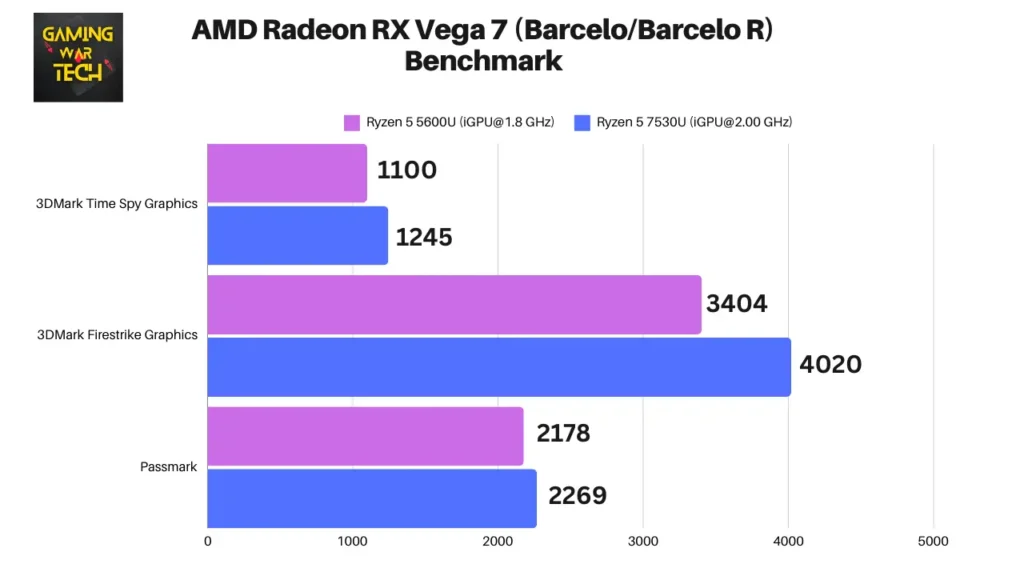
| Benchmark Tools | Ryzen 5 5600U (Radeon RX Vega 7 at 1.8 GHz) | Ryzen 5 7530U (Radeon RX Vega 7 at 2.0 GHz) |
|---|---|---|
| 3DMark Time Spy Graphics | 1100 | 1245 |
| 3DMark Firestrike Graphics | 3404 | 4020 |
| Open CL | No Data | No Data |
| Vulkan | No Data | No Data |
| Passmark | 2178 | 2269 |
Gaming Performance
Gaming performance is to measure how well this integrated graphics card performs in gaming by running multiple games on it and calculating the average fps and 1% lows.
Gaming Benchmark on Ryzen 5 5600U iGPU clocked at 1.80 GHz
The gaming benchmark is from the Ryzen 5 5600U integrated GPU, which is AMD Radeon graphics (igpu) 7cu/448SP 1.80GHz.
The Test System is the HP Pavilion Aero 13 (4H3H8EA) with Ryzen 5 5600U and RX Vega 7 onboard graphics, 16GB DDR4-3200 MHz RAM, 1TB SSD, and Win 10 PRO.
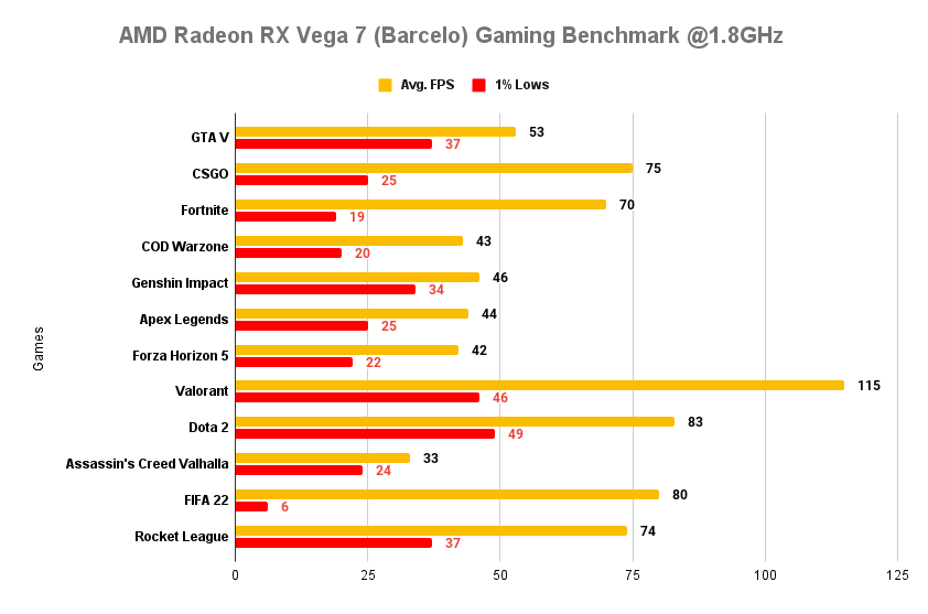
Gaming benchmark details in table format
| Games | Avg. FPS | 1% Low | Graphics Setting |
|---|---|---|---|
| GTA V | 53 | 37 | 1080p, Normal |
| CSGO | 75 | 25 | 1080p, Low |
| Fortnite | 70 | 19 | 1080p, Perf Mode, Tex. = Med, View Dist = Far |
| COD Warzone | 43 | 20 | 1080p, Low, Ren. Res 66% |
| Genshin Impact | 46 | 34 | 1080p, Low |
| Apex Legends | 44 | 25 | 900p, Low |
| Forza Horizon 5 | 42 | 22 | 900p, Low/Med |
| Valorant | 115 | 46 | 1080p, Low |
| Dota 2 | 83 | 49 | 1080p, Low |
| Assassin’s Creed Valhalla | 33 | 24 | 720p, Low Res 90% |
| FIFA 22 | 80 | 6 | 1080p, Low |
| Rocket League | 74 | 37 | 1080p, Perf |
Gaming Benchmark on Ryzen 5 7530U iGPU clocked at 2.00 GHz
The gaming benchmark is from the Ryzen 5 7530U integrated GPU, which is AMD Radeon graphics (igpu) 7cu/448SP 2.00GHz.
The Test System is the Acer Swift Go 14 SFG14-41 with Ryzen 5 7530U and RX Vega 7 i-GPU, 16GB LPDDR4X-4266 MHz RAM, 512GB SSD, and Win 11.
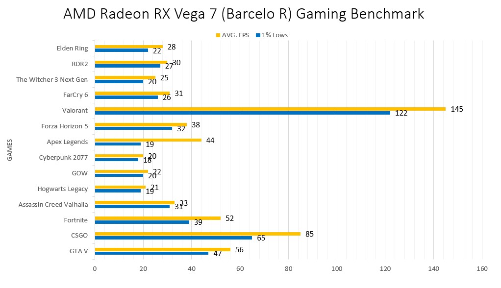
Gaming benchmark details in table format
| Games | Avg. FPS | 1% Low | Graphics Setting |
|---|---|---|---|
| GTA V | 56 | 47 | 1080p, Normal |
| CSGO | 85 | 65 | 1080p, Low/Med |
| Fortnite | 52 | 39 | 1080p, Low |
| Assassin Creed Valhalla | 33 | 31 | 1080p, Low, Res. Scale 70% |
| Hogwarts Legacy | 21 | 19 | 1080p, Low FSR Ultra Perf |
| GOW | 22 | 20 | 1080p, Low FSR Bal |
| Cyberpunk 2077 | 20 | 18 | 1080p, Low FSR Bal |
| Apex Legends | 44 | 19 | 1080p, Low |
| Forza Horizon 5 | 38 | 32 | 1080p, Low |
| Valorant | 145 | 122 | 1080p, High |
| FarCry 6 | 31 | 26 | 1080p, Low, Res. scale 70% |
| The Witcher 3 Next Gen | 25 | 20 | 1080p, Lowest |
| RDR2 | 30 | 27 | 1080p, Low FSR Bal |
| Elden Ring | 28 | 22 | 1080p, Low |
Is the AMD Radeon RX Vega 7 good for gaming?
1080p Low gaming is possible with AMD Radeon RX Vega 7. However, I suggest you also use FSR to get decent playable framerates. Without using FSR 1080p gaming is a bit laggy.
You can lower your gaming resolution to 900p on games that seem unplayable.
What is the Radeon RX Vega 7 Nvidia equivalent?
Radeon RX Vega 7 easily beats the Nvidia MX230 mobile dedicated GPU and is equivalent to the Nvidia Geforce MX250 in terms of performance on a notebook.
Regarding desktops, the AMD Radeon RX Vega 7 GPU beats the Nvidia GTX 460, is equivalent to the GTX 650, and slightly gets beaten out by a 4% margin.
AMD Radeon Vega 7 (Barcelo) GPU Used in Following CPUs
| Processors | GPU Base Clock | GPU Boost Clock | FP32(Float) |
|---|---|---|---|
| Ryzen 5 5625U | 300 MHz | 1.80 GHz | 1.612 TFLOPS |
| Ryzen 5 5600U | 300 MHz | 1.80 GHz | 1.612 TFLOPS |
| Ryzen 5 PRO 5675U | 300 MHz | 1.80 GHz | 1.612 TFLOPS |
| Ryzen 5 PRO 5650U | 300 MHz | 1.80 GHz | 1.612 TFLOPS |
| Ryzen 5 7530U | 300 MHz | 2.00 GHz | 1.792 TFLOPS |
| Ryzen 5 PRO 7530U | 300 MHz | 2.00 GHz | 1.792 TFLOPS |


